只用于动物实验研究等 PFN is a conjugated polyelectrolyte used as an electron-interface in OPV devices to improve extraction efficiencies. Currently producing power conversion efficiencies of up to 7.1% at Ossila with further increases expected from additional optimisation and up to 9.2% reported in the literature [1-3]. Soluble in polar solvents such as water and methanol in the presence of small amounts of acetic acid. 代理Ossila材料PFN CAS:673474-74-3 General Information| Full name | Poly [(9,9-bis(3'-(N,N-dimethylamino)propyl)-2,7-fluorene)-alt-2,7-(9,9–dioctylfluorene)] | | Synonyms | PFN | | Chemical formula | (C52H70N2)n | | CAS number | 673474-74-3 |
 Chemical structure of PFN. CAS no.: 673474-74-3. Chemical formula: (C52H70N2)n. Chemical structure of PFN. CAS no.: 673474-74-3. Chemical formula: (C52H70N2)n.
代理Ossila材料PFN CAS:673474-74-3 Usage detailsInverted OPV devices were made using the architecture shown below with PFN (batch M221) as an electron-interface and PTB7:PC70BM in a 1:1.5 blend ratio (batches M211 and M113 respectively). Ossila's S173 pixelated cathode substrate pack provided the device components. Glass / ITO (100 nm) / PFN (5.5 to 10 nm) / PTB7:PC70BM (90 nm) / MoOx (15 nm) / Al (100 nm) The substrate cleaning and PFN spin-coating were performed under ambient conditions with all other steps performed in an N2 glovebox until encapsulation had been completed (measurement performed under ambient conditions). For generic details please see the fabrication guide and video. For specific details please see the condensed fabrication routine shown below. For information on our inexpensive Spin Coater for use with PFN please see our Spin Coater product page. The active layer thickness, MoOx thickness, cathode metal (Ag or Al), PFN solution concentration, PFN drying/baking have not been fully optimised. As such, we expect further gains to be made with additional engineering work. However, for the devices made in this fabrication, a peak efficiency of 7.1% was achieved.  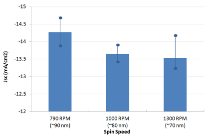 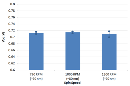 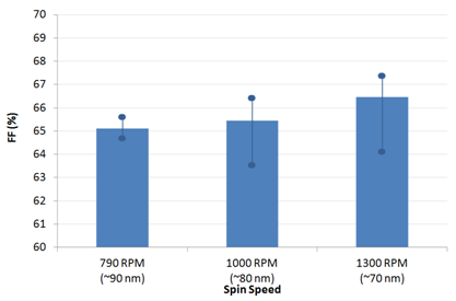 Figure 1: PCE, Jsc, Voc and FF for different spin speeds. Data shown is averaged with max and min overlaid with filled circles. Figure 1: PCE, Jsc, Voc and FF for different spin speeds. Data shown is averaged with max and min overlaid with filled circles.

Figure 2: The JV curve for the best performing device.
Note that some burn-in was observed (i.e. a small improvement in device performance after a few seconds under the solar simulator) and the variability of the devices is currently slightly higher than for other interlayers (average PCE of 6.7%). We expect the uniformity to improve with further improvements in PFN processing, in particular the optimisation of drying conditions to ensure that the acetic acid is fully removed prior to active layer deposition. Fabrication RoutineThe below fabrication routine was used to fabricate inverted solar cells with peak efficiency of 7.1%. Further gains are expected with further optimisation. Substrates/Cleaning: - Pixelated Cathode substrates (S173)
- 5 mins sonication in hot Hellmanex III (1 ml in beaker)
- 2x boiling water dump rinses
- 5 mins sonication in warm IPA
- 2x dump rinses
- 5 mins sonication in hot NaOH
- Dump rinse in boiling water
- Dump rinse in water
- Stored in DI water overnight and until use
PFN solution: - Stock solution of acetic acid dissolved 1:9 in methanol to enable low concentration solutions to be made more easily.
- Acetic acid solution further dissolved to produce 2 μl/ml solution.
- PFN dissolved at 2 mg/ml in methanol with 2 μl/ml of acetic acid with stirbar at ambient temperature for 10 minutes
- Filtered through 0.45 μm PVDF filter
PFN Test Films - PFN Test film initially spun at 500 rpm and gave 21-22 nm
- Second test film spun at 1000 rpm and gave 13-16 nm
- Thicknesses extrapolated for higher spin speeds
- It was noted that at low spin speeds 500 rpm to 2400 rpm there were significant crystallites present in the films - especially on the ITO. Extra filtration showed that this was not due to the solution and therefore most have been due to the drying process
Active Layer Solution - Fresh stock solution of PTB7 made on at 10 mg/ml in CB and dissolved with stirbar for 1 hour (dissolves very easily)
- Mixed 1:1.5 with dry Ossila 95/5% C70 PCBM to make overall concentration of 25 mg/ml and dissolved with stirbar for 1 hour more
- 3% of diiodooctane (DIO) added to solution
- Filtered using 0.45 μm PVDF syringe filter
Active Layer Test Films - Test film spun at 1000 rpm for 2 mins using unfiltered solution and thickness measure on Dektak. Note that films must be fully dry before performing Dektak measurements.
- 1000 rpm gave approximay 90 nm thickness.
Active layers - Devices spun using 30 μl dynamic dispense (20 μl gave only moderate wetting/coverage)
- Spun for 2 mins
- Cathode wiped with CB
- Vacuum dried in glovebox anti-chamber for 20 mins to remove residual DIO from films
Cathode Evaporation - 15 nm of MoOx evaporated at 0.2 Å/s from fresh pellets at pressure <1e-6 mbar="" li="">
- 100 nm of Al evaporated at 1.5 Å/s at pressure <1e-6 mbar="" li="">
Annealing / Encapsulation - No annealing performed
- Encapsulated as standard, using Ossila EE1 (E131) epoxy and glass coverslip (C181) (30 mins in UV box).
Measurements - JV sweeps taken with Keithley 237 source-meter
- Illumination by Newport Oriel 9225-1000 solar simulator with 100 mW/cm2 AM1.5 output
- NREL certified silicon reference cell used to calibrate lamp output
- Lamp current: 7.9 A
- Solar output at start of testing: 0.995 suns at 25°C
- Solar output at end of testing: 1.00 suns at 25°C
- Electrochemically etched aperture mask was optically calibrated to 0.212 cm2
ReferencesPlease note that Ossila has no formal connection to any of the authors or institutions in these references. - Enhanced power-conversion efficiency in polymer solar cells using an inverted device structure, Z. He et al., Nature Photonics, 6, 591–595 (2012)
- Simultaneous Enhancement of Open-Circuit Voltage, Short-Circuit Current Density, and Fill Factor in Polymer Solar Cells, Z. He et al., Advanced Materials, 23, 4636–4643 (2011)
- Investigation of a Conjugated Polyelectrolyte Interlayer for Inverted Polymer:Fullerene Solar Cells, R. Xia et al., Advanced Energy Materials, (2013)
To the best of our knowledge the technical information provided here is accurate. However, Ossila assume no liability for the accuracy of this information. The values provided here are typical at the time of manufacture and may vary over time and from batch to batch. |


 发送消息
发送消息